Clock Distribution
LimeSDR Mini board clock distribution block diagram is as shown in Figure 7.
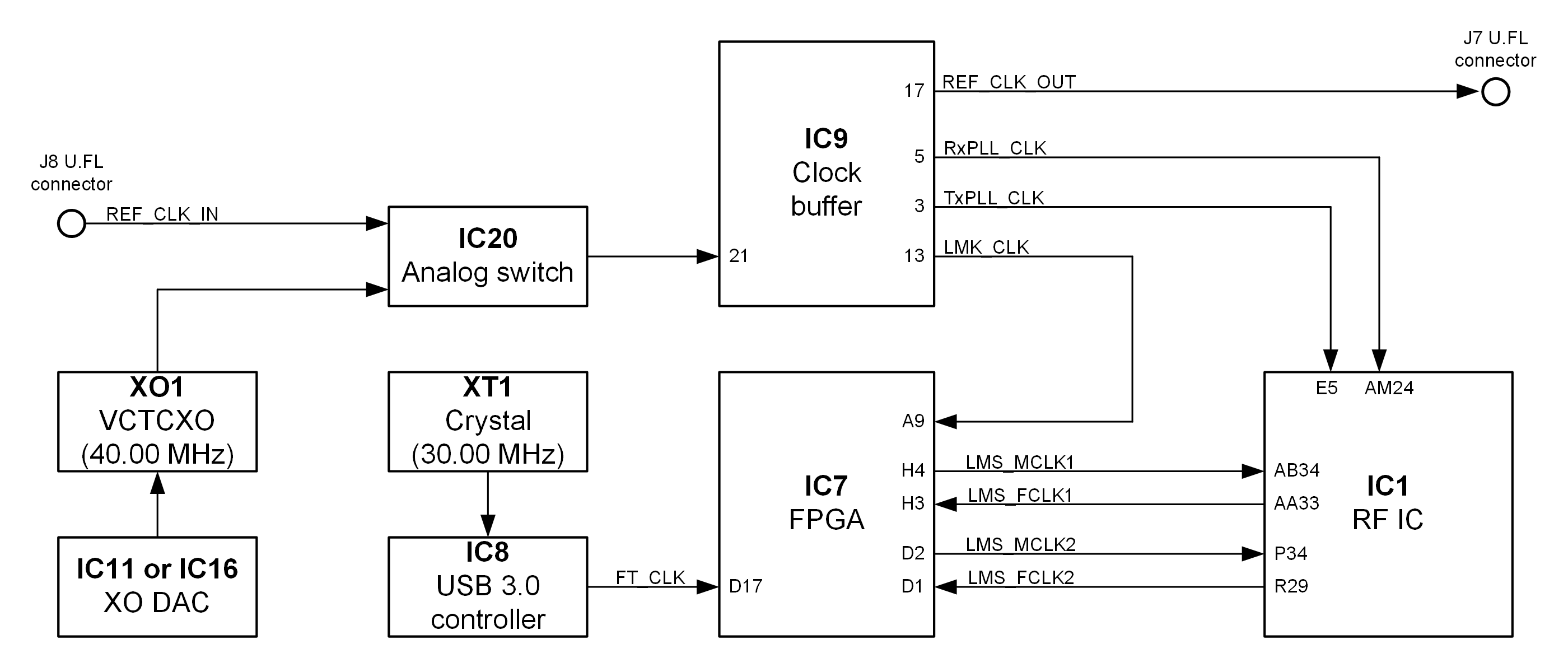
Figure 7. LimeSDR Mini v2.4 board clock distribution block diagram
LimeSDR XTRX board features an on board 40.00 MHz VCTCXO as the reference clock for LMS7002M RF transceiver and FPGA PLLs.
Rakon E7355LF 40 MHz voltage controlled temperature compensated crystal oscillator (VCTCXO) is the clock source for the board. VCTCXO frequency can be tuned by using 10 bit (IC11) or 16 bit (IC16 unpopulated) DAC. Main VCTCXO parameters are listed in Table 5.
Frequency parameter |
Value |
|---|---|
Calibration (25°C ± 1°C) |
± 1 ppm max |
Stability (-40 to 85 °C) |
± 0.5 max |
Long term stability (1 year, 10 years) |
± 2 ppm max, ± 4 ppm max |
Control voltage range |
0.5 V .. 2.5 V |
Frequency tuning |
± 7 ppm min, ± 15 ppm max |
Slope |
+9 ppm/V |
Analogue switch gives option to select clock source for RF transceiver and FPGA from buffered onboard VCTCXO clock (XO1) and external U.FL (J8). Buffered clock output (REF_CLK_OUT) is also available using U.FL (J7) connector.
The board clock lines and other related signals/information are listed in Table 6.
Source |
Schematic signal name |
I/O standard |
FPGA pin |
Description |
|---|---|---|---|---|
External |
REF_CLK_IN |
2.5V/3.3V |
External reference clock input |
|
Clock buffer (IC9) |
REF_CLK_OUT |
3.3V |
Reference clock output |
|
Clock buffer (IC9) |
LMK_CLK |
3.3V |
A9 |
Reference clock connected to FPGA |
RF transceiver (IC1) |
RxPLL_CLK |
1.8V |
Reference clock input |
|
TxPLL_CLK |
1.8V |
Reference clock input |
||
LMS_MCLK1 |
2.5V/3.3V |
H4 |
||
LMS_FCLK1 |
2.5V/3.3V |
H3 |
||
LMS_MCLK2 |
2.5V/3.3V |
D2 |
||
LMS_FCLK2 |
2.5V/3.3V |
D1 |
||
USB 3.0 controller (IC8) |
FT_CLK |
3.3V |
D17 |
Clock output (100 MHz) from USB controller |