Overview
The heart of the LimeSDR-Mini board is Lattice ECP5 (LFE5U-45F) FPGA. It’s main function is to transfer digital data between the LMS7002M RF transceiver and a PC through a USB 3.0 connector. The block diagram for LimeSDR-Mini board is presented in the Figure 3.
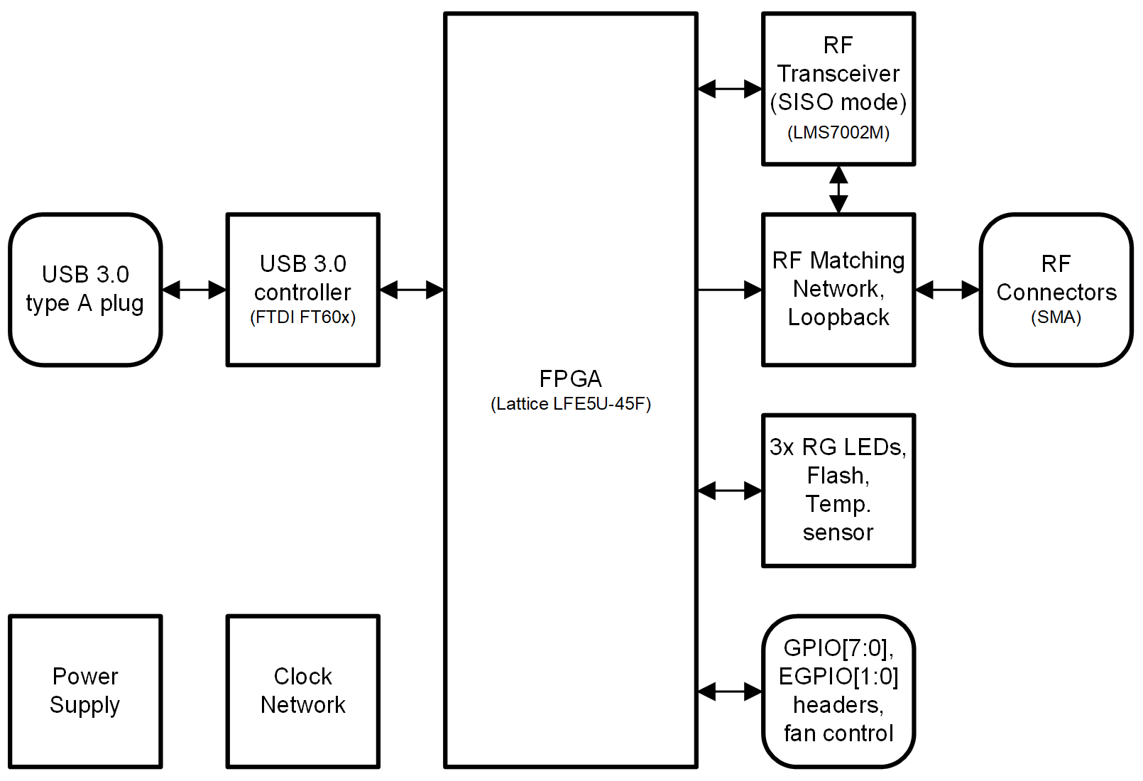
Figure 3: LimeSDR Mini v2.2 board block diagram
This section contains component location description on the board. LimeSDR Mini v2.2 board picture with highlighted connectors and main components are presented in Figure 4 and Figure 5, respectively.
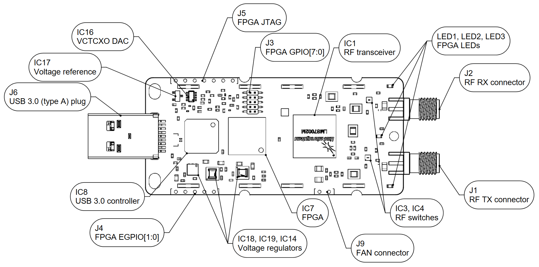
Figure 4: LimeSDR Mini v2.2 board top connectors and main components
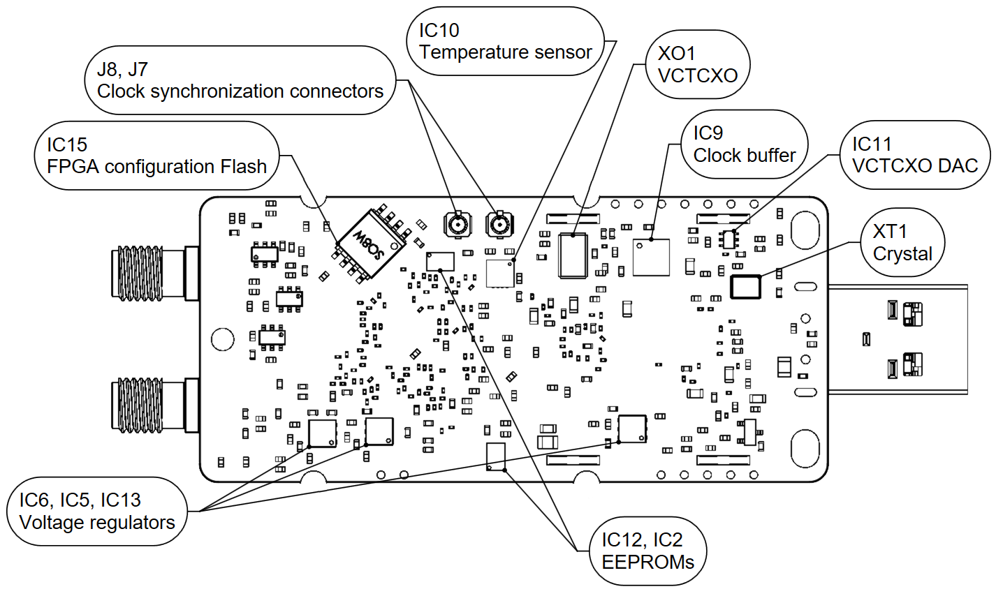
Figure 5: LimeSDR Mini v2.2 board bottom connectors and main components
Description of board components is given in the Table 1.
Featured Devices |
||
Board Reference |
Type |
Description |
IC1 |
RF transceiver |
Lime Microsystems LMS7002M |
IC7 |
FPGA |
Lattice Semiconductor’s LFE5U (LFE5U-45F) |
IC8 |
USB 3.0 microcontroller |
FTDI USB 3.0 to FIFO interface bridge chip FT601 |
Miscellaneous devices |
||
IC10 |
IC |
Temperature sensor LM75 |
Configuration, Status and Setup Elements |
||
J5 |
JTAG chain connector |
FPGA programming pin header on the board edge for JTAG cable, 0.1” pitch |
LED1, LED2, LED3 |
Red-green status LEDs |
User defined FPGA indication LED. |
General User Input/Output |
||
J3 |
Pin header |
8x FPGA GPIOs, 3.3V, 0.05” pitch |
J4 |
Pin header |
2x FPGA GPIOs on the board edge, 3.3V, 0.1” pitch |
J9 |
Pin header |
5V (3.3V voltage can be chosen by resistors) fan connection pin headers, 0.1” pitch |
Memory Devices |
||
IC2 |
IC |
I²C EEPROM Memory 128Kb (16 x 8), connected to RF transceiver I2C bus |
IC12 |
IC |
I²C EEPROM Memory 128Kb (16K x 8), connected to FPGA I2C bus |
IC15 |
IC |
Quad SPI Flash Memory 128 Mb (16M x 8) connected to FPGA SPI |
Communication Ports |
||
J6 |
USB 3.0 connector |
USB 3.0 (type A) plug |
Clock Circuitry |
||
XO1 |
VCTCXO |
40.00 MHz Voltage Controlled Temperature Compensated Crystal Oscillator |
IC11 |
IC |
10 bit DAC for TCXO (XT4) frequency tuning (default) |
IC16 |
IC |
16 bit DAC for TCXO (XT4) frequency tuning (unpopulated) |
IC17 |
IC |
Voltage reference (unpopulated) |
IC9 |
IC |
Clock buffer |
IC20 |
IC |
Analog switch |
J8 |
U.FL connector |
Reference clock input |
J7 |
U.FL connector |
Reference clock output |
Power Supply |
||
IC14 |
IC |
Switching regulator LMZ10501 (1.8V rail) |
IC19 |
IC |
Switching regulator LMZ10501 (3.3V rail) |
IC13 |
IC |
Linear regulator LD39100PUR (1.1V rail) |
IC5 |
IC |
Linear regulator LD39100PUR (1.25V rail) |
IC6 |
IC |
Linear regulator LD39100PUR (1.4V rail) |
IC18 |
IC |
Linear regulator LD39100PUR (2.5V rail) |
A more detailed description is provided in the following sections.